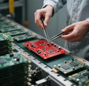
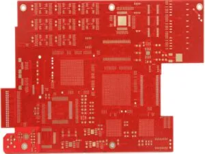
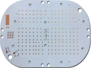
HDI PCB is the abbreviation of High Density Interconnect Printed Circuit Board. HDI PCB is characterized by having very precise and small circuits. It usually needs to use 0.2mm buried holes and 0.1-0.05mm laser blind holes to conduct each layer of circuits.
What defines a HDI PCB board?
IPC-2226 defines HDI as a printed circuit board with a higher wiring density per unit area than conventional printed circuit boards (PCB). They have finer lines and spaces ≤ 100 µm / 0.10mm, smaller vias (<150 µm) and capture pads <400 µm / 0.40mm, and higher connection pad density (>20 pads/cm2) than employed in conventional PCB technology.
HDI PCB Manufacturing Capabiltiy :
1+N+1, 2+N+2, 3+N+3,4+N+4, ELIC HDI PCB

ELIC HDI PCB Manufacturing
ELIC (Every Layer InterConnect).All the layers of a PCB are high-density interconnection layers, which allows the conductors on any layer of the PCB to be interconnected freely with copper-filled stacked microvia structures (“any layer via”). This provides a reliable interconnect solution for highly complex, large pin count devices, such as central processing unit (CPU) and graphics processing unit (GPU) chips utilized on handheld and mobile devices.
As a leading HDI PCB supplier, we supply various types and sizes of high-density interconnect PCBs.
Suitable HDI surface finishes: ENIG, Lead Free HASL, Immersion Silver, Immersion Tin, OSP, ASIG, ISIG.
Suitable HDI Materials available: Standard TG FR4, High TG FR4, Taconic, Rogers, Arlon, Nelco, Isola, Halogen free FR4.
Via fill options: Resin Fill via, Copper plated shut up to max 6L, Solder mask ink.
For more information on our HDI printed circuit boards, get in touch with a member of our expert team.
Quick turn: 8-10 days
Prototype and mall series production: 2-3 weeks
Mass production: 3-4 weeks
Request HDI PCB manufacturing quotation, Please send PCB files to Sales@pcba123.com