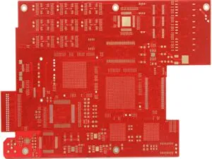
HDI PCB Prototype is a preliminary version of a High-Density Interconnect circuit board, designed for compact, high-performance electronics.
Key Features of HDI PCB Prototypes
Ultra-Fine Circuitry
Trace Width/Spacing: As small as 3 mil (0.076 mm) – 5× finer than standard PCBs.
Microvias: Laser-drilled holes (0.1–0.15 mm diameter) connecting layers, enabling complex routing.
Blind/Buried Vias: Vias hidden between inner layers, saving surface space.
High Layer Density Circuit board.
Stacked Microvias: Multiple microvias stacked vertically to link 3+ layers (e.g., 6-step HDI in Nvidia AI servers).
Thin Dielectrics: Layers as thin as 0.05 mm for slimmer boards (e.g., foldable smartphones).
Enhanced Signal Integrity
Impedance Control: Tight tolerance (±5%) for high-speed signals (critical for 5G/AI).
Low-Loss Materials: Specialty laminates (e.g., Rogers, Megtron) reducing signal distortion.
Prototyping Cost & Lead Time
| Complexity | Quick turn Lead Time | |
| 4–6 layers (basic) | 5-7 Days | |
| 8–12 layers (AI/5G) | 8–10 days | |
| 12+ layers (advanced) | 10–14 days |
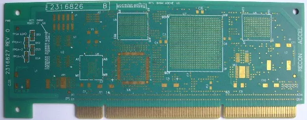
Why HDI PCB prototype have competitive cost in China?
China’s competitive cost structure for HDI (High-Density Interconnect) PCB prototypes stems from a confluence of industrial, technological, and strategic factors. Below is a detailed analysis:
1. Industrial Cluster and Supply Chain Efficiency
Manufacturing Scale: China dominates global HDI production, accounting for 62% of global HDI output (2021), with clusters in the Pearl River Delta facilitating streamlined material procurement and logistics .
Localized Supply Chains: Domestic availability of raw materials (e.g., specialty copper-clad laminates from Shengyi Technology) and equipment reduces import dependency and tariffs. For example, Chinese manufacturers leverage local suppliers for high-speed laminates, avoiding 15-20% import premiums.
Equipment Redundancy: Past industry over-expansion (2020-2021) left idle advanced machinery (e.g., laser drilling systems), allowing smaller players to access high-end capabilities at lower entry costs.
2. Technological Maturity and Yield Optimization
Process Innovation: Companies like Shennan and PCBA123 achieve >99% rate for high-end HDI PCB (e.g., 6step with 24 layers boards), reducing waste and rework costs.
Automation Adoption: Automated optical inspection (AOI) and laser direct imaging (LDI) systems cut labor needs by 30%, compressing prototyping time to 24-72 hours.
3. Labor and Operational Economics
Skilled Labor Cost: Despite automation, labor constitutes 20-25% of prototype costs. China’s engineering wages remain 40-50% lower than in Taiwan/South Korea.
High-Mix Flexibility: HDI PCB Prototype-focused fabs (e.g., Hitech Circuits) operate dedicated quick-turn lines with <10 panels MOQ, minimizing idle capacity.
China’s HDI PCB prototype cost edge arises from integrated supply chains, policy-enabled scale, and process innovation, though dependency on foreign tech (e.g., ultrafine laser drills) and financial health remain watchpoints. Companies like Hitech Circuits and VGT exemplify this model, offering prototypes at 30-50% below Western quotes while supporting rapid updated.
For sourcing, prioritize vendors with diversified clientele and vertical integration (e.g., Shengyi for materials + VGT for HDI PCB fabrication) to mitigate risks.