Rapid PCB Prototyping refers to the fast-track process of designing, PCB manufacturing, and PCB testing physical printed circuit boards (PCBs) in a very short timeframe – often within 24 hours to a few days. It bridges the gap between initial electronic design and functional validation, enabling engineers and designers to iterate quickly.
Key Aspects of Rapid PCB Prototyping
Speed: The core focus. Traditional PCB fabrication can take weeks. Rapid prototyping slashes this to days or even hours using:
Advanced Manufacturing: Automated processes (direct imaging, automated routing).
Dedicated Service Bureaus: Companies specializing in fast-turn orders (e.g., PCBA123, HITECHPCB, OSH Park, etc.).
Optimized Logistics: Overnight/express shipping options.
Technologies Used:
Subtractive (Most Common): Starts with copper-clad laminate. Uses:
Photolithography & Etching: UV light exposes design on photoresist, chemicals etch away unwanted copper (standard for multi-layer boards).
CNC Milling: Precise routers physically mill away unwanted copper (great for simple 1-2 layer boards, very fast in-house option).
Additive (Emerging): Deposits conductive material (inks, pastes) onto a substrate (e.g., inkjet printing, aerosol jet). Faster for ultra-simple designs but less common/mature for complex boards.
Hybrid: Combines methods (e.g., milled substrate with printed traces).
Primary Methods for Access:
Online PCB Fabrication Services: The dominant method. Upload design files (Gerber), choose options (layers, material, finish), and receive boards via courier in days.
In-House PCB Prototyping Systems: Desktop CNC mills (e.g., Bantam Tools) or small additive printers. Best for very simple 1-2 layer boards overnight in the lab/office.

Typical Turnaround Times:
Standard “Rapid”: 24-72 hours (PCB manufacturing time, excluding shipping).
Expedited: As fast as 8-24 hours (premium cost).
Shipping: Adds 1-5 days depending on location and service chosen.
Key Benefits:
Faster Design Iteration: Test concepts, find errors, and refine designs quickly.
Reduced Development Time & Cost: Catch flaws early before expensive full-scale production.
Lower Risk: Validate functionality, fit, and manufacturability early.
Flexibility: Easy to make design changes between iterations.
Proof of Concept: Quickly demonstrate feasibility to stakeholders.
Small Batch Production: Ideal for very low-volume production runs or niche products.
Common Use Cases:
Functional testing of new circuit designs.
Form factor and fit checks (mechanical validation).
Firmware development and debugging.
Design for Manufacturability (DFM) checks.
Creating demo units or pre-production samples.
Low-volume production for specialized applications.
Factors Affecting Speed & Cost:
Number of Layers: 1-2 layers are fastest/cheapest; 4+ layers add complexity/time.
Board Size & Complexity: Larger boards, dense traces, small vias increase time.
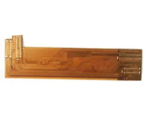
Material: Standard FR-4 is fastest; exotic materials (RF, flex) take longer.
Surface Finish: HASL lead-free is standard/fastest; ENIG, immersion silver add time.
Quantity: Prototype quantities (1-10 boards) are optimized for speed.
Shipping Method: Overnight shipping significantly reduces total lead time.
In essence: Rapid PCB Prototyping is the engine of modern electronics development. It leverages specialized processes and services to transform a digital circuit design into a physical board incredibly fast, enabling rapid innovation, testing, and refinement. It’s fundamental for bringing electronic products to market efficiently.