What is a prototype PCB assembly?
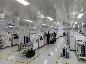
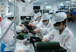
PCB assembly Prototype service can offer one-stop service from PCB manufacturing, components sourcing, PCB assembly, SMT assembly, THT assembly, PCBA testing, product assembly, packaging, and delivery. You are not responsible for or supply any parts on this process and just need to deal with your design while suppliers take care of the rest. And they are without MOQ requirement for your PCBA prototype, just do the quantity you need.
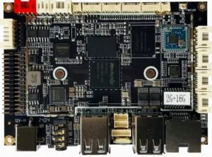
A Prototype PCB Assembly is the process of manufacturing a small batch of printed circuit boards (PCBs) and then populating them with electronic components specifically for the purpose of testing, validation, and refinement of a new electronic design before committing to full-scale mass production.
Here’s a breakdown of its key aspects:
1, Purpose:
Verification: To physically test if the circuit design works as intended.
Validation: To ensure the design meets all functional requirements and specifications.
Debugging: To identify and fix design flaws, component compatibility issues, signal integrity problems, power issues, and manufacturing defects.
Form Factor Testing: To check the physical fit of the PCB within its intended enclosure or system.
Software Development: To provide hardware for developing and testing firmware/software.
Regulatory Testing: To use in pre-compliance testing for certifications (FCC, CE, etc.).
Demonstration: To showcase the product concept to investors, clients, or stakeholders.
2, Key Characteristics for prototype PCB assembly :
Low Volume: Typically involves assembling a very small number of boards (e.g., 1 to 50 units, sometimes up to 100-200).
Focus on Speed & Flexibility: Prioritizes getting functional boards quickly to accelerate the design-test-iterate cycle. Turnaround time is often more critical than per-unit cost at this stage.
Design Changes Expected: The design is not finalized; changes based on prototype testing are anticipated.
Higher Per-Unit Cost: Economies of scale don’t apply. Setup costs (programming machines, stencil creation) are spread over very few units. Manual assembly or specialized low-volume lines are often used.
Component Sourcing Flexibility: May use components from distributors (at higher cost) rather than bulk suppliers. Might involve manual placement of hard-to-source parts.
3, The PCB Assembly Process (Typical Steps for PCBA Prototypes):
PCB Fabrication: Manufacturing the bare printed circuit boards based on the design files (Gerbers).
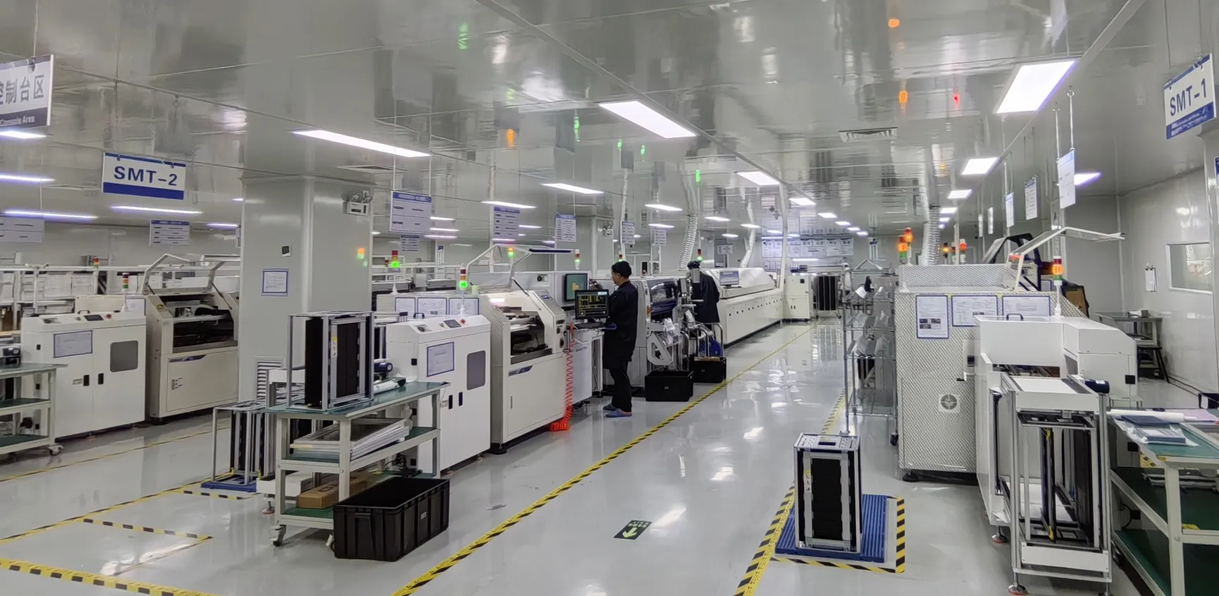
Solder Paste Application: Applying solder paste onto the PCB pads, usually using a stencil (even for prototypes, a laser-cut stencil is common for accuracy).
Component Placement: Placing surface-mount (SMD/SMT) components onto the solder paste. This can be done by:
Automated Pick-and-Place Machine: Faster and more accurate for complex boards, common even for prototypes.
Manual Placement: Used for very simple boards or specific awkward components.
Reflow Soldering: Passing the board through a reflow oven to melt the solder paste and create electrical/mechanical connections for SMD components.
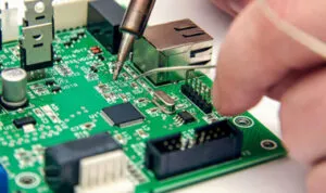
Through-Hole (THT) Component Placement & Soldering: Manually inserting components with leads into holes and soldering them (often using a soldering iron or selective wave soldering).
4, Inspection & Testing:
Automated Optical Inspection (AOI): Checks for component presence, polarity, and basic solder joint quality.
X-Ray Inspection (AXI): Used for inspecting hidden solder joints (e.g., under BGAs).
Basic Power-On Test: Checks for shorts or obvious failures.
In-Circuit Test (ICT) / Flying Probe Test: Tests individual components and connections (more common in later prototype stages or production).
Functional Test (FCT): Verifies the board performs its intended function.
Debugging & Rework: Fixing any identified issues manually.
Conformal Coating (Optional): Applying a protective layer if required for environmental testing.
5, Why is Prototype PCB Assembly Crucial?
Catches Design Errors Early: Fixing mistakes on a prototype is vastly cheaper and faster than fixing them after thousands of units are manufactured.
Reduces Risk: Mitigates the significant financial and reputational risk associated with launching a faulty product.
Validates Manufacturing: Helps identify potential manufacturing challenges before scaling up.
Accelerates Development: Enables rapid iteration cycles (design -> prototype -> test -> improve).
Saves Money in the Long Run: The upfront cost of prototyping is an investment that prevents much larger costs later.
In essence: Prototype PCB Assembly bridges the gap between a theoretical circuit design (on paper or in CAD) and a fully functional, manufacturable electronic product. It’s an essential, iterative step in responsible electronics development to ensure the final product works correctly, reliably, and can be efficiently manufactured.
Prototype PCB assembly bridges design validation and full-scale production, minimizing risks of costly errors in final products.
Hitechpcba provides Prototype PCB Assembly Service offers fast, high-quality PCB assembly for prototypes and small batches.
Key Features:
✅ Quick Turn around – 24-72hrs for PCB fabrication + 3-7 days for PCB assembly.
✅ Advanced Tech Support – Handles BGA, QFN, 01005 components with precision.
✅ Full Testing – Includes AOI, flying probe, and functional testing (optional).
✅ Low MOQ – Supports 1-piece prototypes to mid-volume production.
✅ Global Shipping – Fast delivery to US, EU, and Asia.
Good for: Engineers, startups, and businesses needing reliable, fast-turn PCB assembly with testing options.