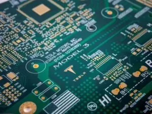
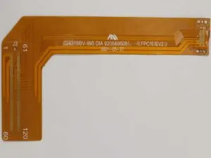
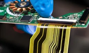
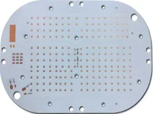
Halogen Free PCB (Printed Circuit Board, HF PCB) refers to a circuit board manufactured without the use of halogen elements (fluorine, chlorine, bromine, iodine) in its materials, particularly in substrates, laminates, solder masks, and inks. This design adheres to environmental and safety regulations aimed at reducing toxic hazards. Below is a detailed breakdown:
1. Halogens in PCBs: Purpose and Risks
Purpose:
Halogens like bromine (Br) and chlorine (Cl) are commonly used as flame retardants (e.g., TBBP-A, PBDEs) in epoxy resins, solder masks, and laminates. They help PCBs meet fire-safety standards (e.g., UL94V-0) by raising ignition temperatures to ~300°C.
Risks:
Toxic emissions: When burned, halogens release dioxins (carcinogenic) and corrosive gases (e.g., hydrogen bromide), endangering health and equipment.
Environmental persistence: Compounds like brominated flame retardants (BFRs) accumulate in ecosystems and resist degradation.
2. Halogen-Free PCB Standards
PCBs are deemed “halogen-free” if they meet these limits (per IEC 61249-2-21):
| Halogen | Max Limit (ppm) | Notes |
|---|---|---|
| Bromine (Br) | 900 | Total across all materials |
| Chlorine (Cl) | 900 | Excludes non-hazardous forms |
| Br + Cl | 1,500 | Cumulative limit |
| Fluorine, iodine, and astatine are typically unregulated due to lower risks. |
3. Key Material Changes
Flame retardant alternatives:
Phosphorus-based compounds: React chemically with resins for heat resistance but may cause river pollution (eutrophication) .
Metal hydroxides (e.g., aluminum/magnesium hydroxide): Decompose endothermically to cool surfaces, though they require high loading .
Nitrogen-based additives: Less efficient but environmentally safer.
Eliminated substances:
Brominated epoxy resins, PVC coatings, and halogenated solder masks.

4. Challenges in Adoption
Reliability concerns:
Halogen-free laminates may suffer lower thermal stability and moisture absorption, risking delamination during lead-free soldering (high-temperature reflow at 260°C+) .
Cost and compatibility:
Alternative materials cost 10–30% more and require rigorous validation of electrical properties (e.g., dielectric constant) for high-frequency applications .
5. Industry Drivers
Regulations:
EU directives (e.g., RoHS recasts), Norwegian PoHS (banning HBCDD/TBBPA), and corporate policies (e.g., Apple, Dell) enforce halogen-free timelines.
Testing protocols:
Methods like ion chromatography (IEC 62321-3-2) and X-ray fluorescence (XRF) verify compliance .
6. Terminology Clarification
Halogen-Free PCB vs. Halide-Free:
Halogen-free PCB: Excludes all halogen compounds (covalent or ionic).
Halide-free: Only bans ionic halides (e.g., chlorides in fluxes). Thus, halogen-free implies halide-free, but not vice versa.
7. Future Trends
“Green trifecta”: Demand for combined lead-free, halogen-free, and phosphorus-free PCBs is rising, though balancing safety, cost, and eco-friendliness remains challenging.
In summary, halogen free PCBs replace toxic halogens with safer alternatives to meet environmental and health standards, driven by regulations and corporate sustainability goals. Their adoption requires careful material selection and reliability testing to ensure performance parity with traditional PCBs. For deeper technical insights, refer to the cited sources.