What is PCB Prototype?
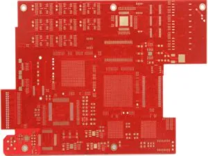
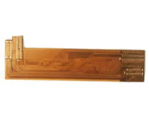
A PCB Prototype is a preliminary, functional sample of a Printed Circuit Board (PCB) created to test and validate the design before committing to full-scale manufacturing. It’s essentially a “draft version” of the final board used for electronics.
Here’s a breakdown of what it is and why it’s crucial:
Purpose & Core Idea:
Test the Design: Verify that the circuit works electrically as intended (connections, signals, power).
Validate Layout: Check component placement, routing, physical dimensions, and fit within the enclosure.
Identify Errors: Catch design flaws (schematic mistakes, footprint errors, routing issues, signal integrity problems, thermal issues) early when they are cheap and easy to fix.
Functional Testing: Program microcontrollers, test sensors, measure performance under real-world conditions.
Refine & Iterate: Make necessary design changes based on PCB prototype testing results.
PCB Prototype Key Characteristics:
Low Volume: Typically only a few boards (e.g., 1 to 10, sometimes up to 50-100) are manufactured initially.
Speed Over Cost (Initially): While cost is always a factor, the primary goal for the first prototype is fast turnaround to get feedback quickly. Costs become more critical in later stages.
May Use Slightly Different Processes: Prototype shops often specialize in rapid fabrication using processes optimized for small batches, which might differ slightly from high-volume mass production lines.
Not for End Users: These boards are for engineers, designers, and testers, not for sale to customers.
Common Types of PCB Prototypes (Progressing Fidelity):
Visual/Mechanical Models: Non-functional, used only to check physical size, shape, hole placement, and component footprint positions. Made quickly and cheaply (sometimes just the bare board).
Breadboard Prototype: Hand-wired circuits on a solderless breadboard, useful for initial schematic validation but doesn’t test the actual PCB layout, signal integrity, or power handling.
“Works-Like” Prototype: Focuses only on electrical functionality. May look rough (e.g., manually soldered, wires hanging off) but proves the core circuit works. Often uses breakout boards/modules.
“Looks-Like/Works-Like” Prototype: A fully assembled PCB prototype using the intended components and manufactured board. This is the most common type people refer to as a “PCB Prototype.” It tests both form and function.
Engineering Validation Test (EVT) / Design Validation Test (DVT) Prototypes: More refined stages where prototypes undergo rigorous functional, environmental, and reliability testing to ensure the design meets all specifications. Closer to the final product.
Pre-Production / Pilot Run: A larger batch (e.g., 100-1000) manufactured using the final intended production process and components, used for final qualification and sometimes early market release.

The PCB Prototyping Process:
Design Completion: Finish the schematic and PCB layout using CAD software (e.g., KiCad, Altium, Eagle).
Generate Manufacturing Files: Create Gerber files (for layers), drill files, pick-and-place files, BOM (Bill of Materials).
PCB Prototype Fabrication Order: Send files to a PCB prototype manufacturer. Options range from:
In-House: Using milling machines or chemical etching (common for very simple, single-layer boards in labs/hobbyist settings).
Online Quick-Turn Services: Specialized companies (like PCBA123, HITECHCPCB, Hitech Circuits, OSH Park, Advanced Circuits) offering fast (often 24-72hr fabrication + shipping), low-cost prototypes in small quantities. This is the most common route.
PCB Assembly (Optional but Common):
Manual PCB Assembly: Engineer/hobbyist solders components themselves.
PCB Prototype Assembly Service: Manufacturer populates the board with components (often for an additional fee, especially for SMT).
Testing & Debugging: Power it up! Use multimeters, oscilloscopes, logic analyzers, software debuggers to test functionality, find bugs, measure performance.
Design Revision: Based on test results, modify the schematic and/or PCB layout.
Repeat: Order new prototypes of the revised design (iteration).
Why PCB Prototyping is Essential (The “Why”):
Catastrophic Cost Avoidance: Fixing a design error found after mass production can cost orders of magnitude more than fixing it in the prototype stage (scrap, rework, recalls).
Saves Time: Identifies problems early, preventing delays later in the production schedule.
Improves Reliability: Thorough testing uncovers issues like noise, crosstalk, thermal hotspots, or mechanical stress that might cause field failures.
Verifies Manufacturability: Ensures the design can actually be built reliably at scale.
Enables Innovation & Refinement: Allows designers to experiment, optimize, and improve the design before locking it down.
Investor/Demonstration Proof: Provides tangible proof of concept for stakeholders or potential customers.
In short: A PCB prototype is a vital step in electronics development. It’s a small batch of boards made to rigorously test and refine the design, ensuring the final mass-produced product works correctly, reliably, and cost-effectively. Skipping PCB prototyping is extremely risky and almost always leads to much higher costs and delays down the line.