
Date: October 11–14, 2026Venue: 2026 Global Sources Electronic Components Exhibition in Hong Kong AsiaWorld – Expo.Booth: 11U14Іnduѕtrу: Еlесtrоnісѕ Component, PCB, PCB Assembly About Global Sources Electronic Components Dive into the

Date: October 11–14, 2026Venue: 2026 Global Sources Electronic Components Exhibition in Hong Kong AsiaWorld – Expo.Booth: 11U14Іnduѕtrу: Еlесtrоnісѕ Component, PCB, PCB Assembly About Global Sources Electronic Components Dive into the
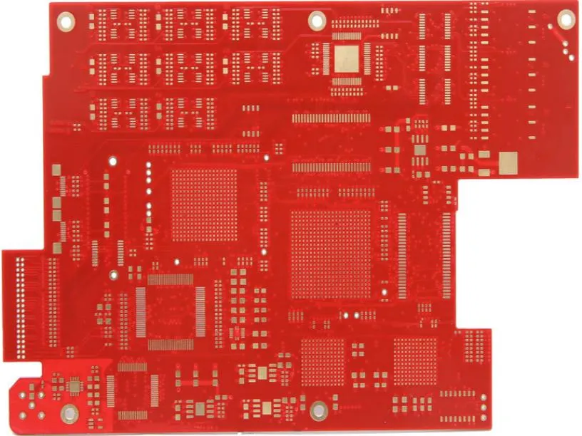
As a PCB circuit board designer, it’s important to understand the basic design flow. This will help you decide the components that will make up your PCB. It also allows you to make sure that your PCB components will be compatible with your overall product. The PCB design process requires collaboration and communication between various stakeholders. It is also crucial to establish timelines and budgets.

PCB layout involves designing a circuit with multiple layers. Some of the fundamental rules of PCB design are as follows: Avoid multiple ground planes. Make analog circuit signals direct and short. Avoid using three distinct capacitors on a single PCB. You can also read our articles on multi-layer PCB design and how to design a multi-layer PCB.
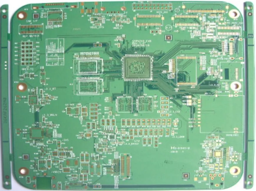
5 Steps to Design a Circuit Board
Designing a circuit board is a complex process. It can be likened to a jigsaw puzzle, which must be arranged in the proper order to produce a functional board. This process involves creating a schematic diagram, calculating impedances, and using a laminating press. Following these steps is an excellent way to create a circuit board that meets all specifications.
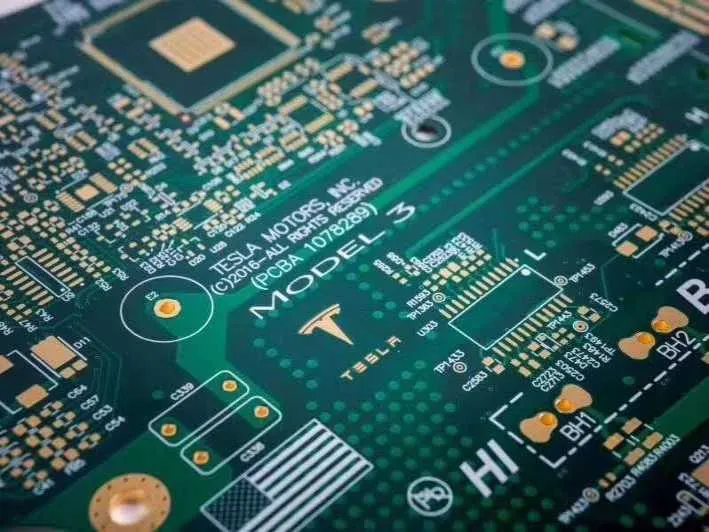
5 Major Causes of Foaming on Copper Plating of a PCB Board
There are many causes of foaming on the copper plating of a PCB board. Some are caused by oil or dust pollution while others are caused by the copper sinking process. Foaming is a problem with any copper plating process as it requires chemical solutions that can cross-contaminate other areas. It can also occur due to improper local treatment of the board surface.
Micro-etching
In micro-etching, the activity of the copper precipitate is too strong, causing pores to leak and blisters. It can also lead to poor adhesion and deteriorate coating quality. Hence, removing these impurities is crucial to prevent this problem.
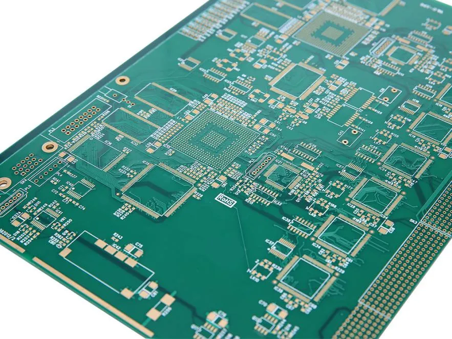
PCB boards are thin boards made of an insulating material coated with metal. The metal is then etched into small patterns that create pathways for electricity to travel. The board is then mounted with various metal components using solder. This makes up a circuit board. There are several different types of PCBs.
Components
When you make a PCB, you should consider the different components that make it up. Every component has its own role to play, but together, they make up a fully functional electrical system. As the creator of a PCB, it is important to use the right ones for the device.
There are many ways to mount the components on a PCB board.

Several factors impact the quality of SMT soldering. These include equipment state, Solder paste quality and Stability. Understanding these factors will help you improve your SMT soldering processes. The best way to improve the quality of SMT soldering is to implement improvements in every area.
Stability
In a manufacturing process where components are placed on a PCB, the stability of the solder joints is important to the performance of the circuit. However, in certain conditions, the soldering process can be unstable. In these conditions, lead-free SnAgCu soldering paste is used to reduce thermal stress on the substrate. This type of solder paste has an advantage over other materials: it can be used on various substrates and can be applied by dispensing the paste onto the device surface.
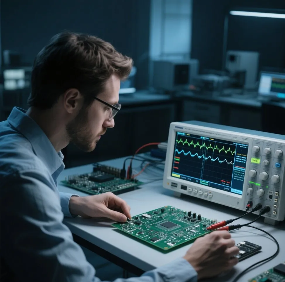
PCB board inspection is a process that involves various tests to find defects. This process involves checking the board for roughness, warpage, and dimensioning. It also involves inspecting the board’s surface quality for defects such as pits, scratches, and voids. In addition, it requires thorough inspection of electrical connectors, vias, and pad plating for defects.
Automated optical inspection (AOI)
AOI is an excellent tool for evaluating the quality of a PCB board. This process can help detect defects in a PCB before they lead to other problems. AOI uses an image processing system to recognize defects. It can also gauge the package’s dimensions.
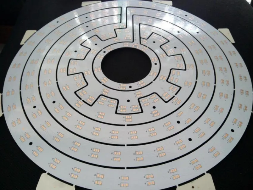
To manufacture a perfect aluminum PCB, there are several steps that you must take. The first step is deciding the stackup and layer count of the PCB. Then, you must choose the materials to be used in different portions of the PCB. Then, you need to decide whether you want to place the aluminum in a core layer or be bonded to the surrounding dielectric layers with a separator membrane. Another option is to have a back-side-mounted plate, or even cutouts.
Processes used to manufacture a perfect aluminum pcb
The aluminum PCB is a common material used in many applications

PCBA123 is a leading manufacturer and supplier of high-quality printed circuit boards for use in the automotive industry, we are known as a trusted and reliable provider of innovative solutions to meet the evolving needs of our customers.
We have a team of experienced professionals who specialize in manufacturing and assembling automotive PCBs, including prototype service, flexible PCBs, multilayer PCBs, and LED PCBs. Our products are designed to provide high performance, reliability, and cost-effectiveness for various electronic systems used in modern vehicles.